The global demand for devices with increasingly faster computing power while reducing power consumption as well as heat dissipation is the key driver of the modern semiconductor industry. To increase transistor density, the size of transistors must be reduced. Current 14-nm/7-nm technology is expected to be replaced in commercial mass production by the 3-nm node in 2022 with the advent of Extreme Ultraviolet (EUV) lithography. Such devices contain more than 100 million transistors per square millimeter, and the actual size of a single transistor approaches that of molecules containing carbon chains of a few atoms. Any impurities can have a detrimental effect on the final product. A clean production environment is therefore of paramount importance to avoid failures during manufacturing.
Background
Solution
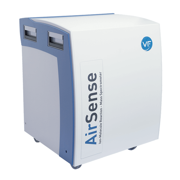
V&F's flagship AirSensemass spectrometer provides real-time analysis with high specificity and ultra-high sensitivity across a broad spectrum (7-519 amu) of contaminants. The proprietary technology is based on ion-molecule reaction mass spectrometry (IMR - MS), a method in which sample molecules are ionized by charge transfer. It can be used to target individual molecules within a gas matrix or to analyze the composition of the matrix over the full range of possible AMCs. Very fast response to concentration changes in the low ppb and sub-ppb range is continuously reported by the software, allowing timely intervention in the relevant process. Typical examples are AMC monitoring in clean rooms, composition at the tool level, and control of outgassing products in Front Opening Universal Pods (FOUP) during wafer transfer.
Advantage
The V&F IMR-MS multicomponent analyzers offer a high degree of automation and are equipped with user-friendly software. The analyzers are characterized by their rapid response time without sample gas conditioning. Their robust design ensures a high degree of stability, minimal downtime, and less maintenance.
learn more
Reference clients (excerpt)


